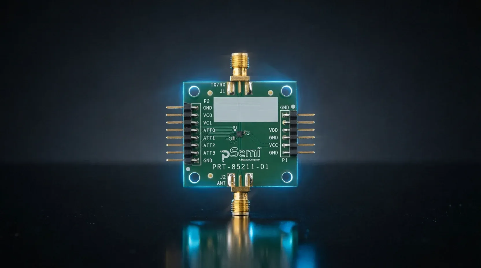
pSemi is targeting the expanding IoT connectivity market by migrating high-performance handset-grade integration into compact, monolithic silicon-on-insulator (SOI) solutions. The company, a Murata subsidiary, has announced the PE566212 and PE566213 front-end modules (FEMs) designed to extend signal range for Bluetooth, Zigbee, and Thread applications. By combining a power amplifier, low-noise amplifier, and RF switch into a single 1.8 mm x 1.8 mm LGA package, pSemi aims to simplify RF design for smart-home, wearable, and wireless-audio hardware developers while providing a silicon-based alternative to traditional GaAs and SiGe technologies.
Expanding UltraCMOS+ Integration to IoT
The introduction of the PE566212 and PE566213 represents a strategic shift for pSemi, applying its patented UltraCMOS+ technology to a new class of connected-device applications. These modules are positioned as fully monolithic solutions that integrate essential RF components—including a power amplifier (PA), low-noise amplifier (LNA), and RF switch—alongside a GPIO control interface. This level of integration is intended to minimize the need for external components, thereby reducing the physical footprint on printed circuit boards.
The company claims these FEMs can provide 5 to 10 times greater range compared to using a standalone System-on-Chip (SoC). This capability is critical for maintaining robust links in complex environments like smart homes or industrial sensing arrays. By leveraging Murata’s manufacturing scale, pSemi is positioning these modules as a reliable, high-volume source for engineers seeking to optimize both transmit and receive performance in space-constrained IoT hardware.
Technical Specifications of PE566212 and PE566213
The two modules offer distinct performance profiles tailored to specific connectivity requirements. Both devices deliver power-efficient transmit output up to +20 dBm and feature a receive noise figure of 1.8 dB at 13 dB of gain. The PE566212 is designed for robust, power-efficient links, supporting Bluetooth Basic Rate Data Rate (BDR) and Bluetooth Low Energy (BLE) with 22.5 dB of transmit digital gain control in 1.5-dB steps.
Conversely, the PE566213 targets throughput-heavy applications such as wireless audio and wearables. While it also supports Bluetooth BDR and BLE up to +20 dBm, it adds support for Bluetooth Enhanced Data Rate (EDR) at up to +11.5 dBm, utilizing 15 dB of transmit digital gain control in 1.0-dB steps. Both modules utilize a 14-lead 1.8 mm x 1.8 mm x 0.63 mm LGA package and maintain a typical bypass-path loss of 0.8 dB, facilitating high-efficiency signal paths for 2.4 GHz protocols.
Key Takeaways
- The PE566212 and PE566213 modules integrate a PA, LNA, and RF switch into a 1.8 mm x 1.8 mm LGA package.
- These FEMs can provide 5 to 10 times more range than a standalone SoC for Bluetooth, Zigbee, and Thread designs.
- The PE566213 specifically supports Bluetooth EDR up to +11.5 dBm for high-throughput applications like wireless audio.
TechInsyte's Take
In our view, pSemi’s move to bring handset-grade SOI integration to the IoT sector is a calculated attempt to disrupt the dominance of GaAs and SiGe in the 2.4 GHz space. By leveraging the UltraCMOS+ process, pSemi is not just offering a component, but a way to bypass the design complexities and footprint penalties associated with discrete RF paths. This signals a broader industry trend where the "intelligence" of the RF front-end is moving toward extreme miniaturization. For enterprise IoT architects, the value proposition lies in the potential for significantly increased range and reduced BOM complexity, provided the silicon-based approach meets the reliability standards required for long-term deployments.
Questions & Answers
How do these modules improve connectivity range for IoT devices?
The modules can provide 5 to 10 times greater range compared to a standalone SoC by integrating a high-performance power amplifier and low-noise amplifier within a monolithic SOI solution.
What is the primary difference between the PE566212 and PE566213 models?
The PE566212 focuses on power-efficient links for BLE and BDR, while the PE566213 is optimized for higher throughput, adding support for Bluetooth EDR up to +11.5 dBm.
What physical footprint should engineers expect for these components?
Both modules are housed in an ultra-compact 14-lead LGA package measuring 1.8 mm x 1.8 mm x 0.63 mm.
Which technologies are these modules intended to replace?
pSemi is positioning these silicon-based FEMs as a highly integrated alternative to traditional Gallium Arsenide (GaAs) and Silicon Germanium (SiGe) front-end solutions.
Source: pSemi