
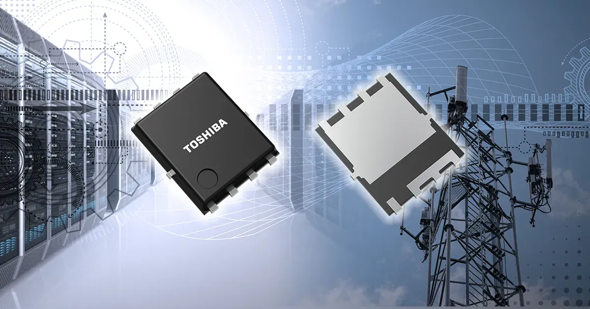
Toshiba Electronic Devices & Storage Corporation has begun shipping TPM1R408RH, an 80 V N‑channel power MOSFET fabricated with the company’s newest U‑MOS11‑H silicon‑process technology. The part is positioned squarely for switched‑mode power supplies (SMPS) that power industrial equipment in AI‑driven data‑centers and the high‑frequency RF front‑ends of communications base stations. As AI workloads continue to push data‑center power consumption upward and next‑generation wireless standards demand ever‑higher efficiency, Toshiba’s latest MOSFET promises to cut both conduction and switching losses while also taming voltage‑spike‑induced electromagnetic interference (EMI). Shipments started in June 2026, and the device is immediately available in Toshiba’s SOP Advance(E) package, which offers markedly lower package and thermal resistance than the prior SOP Advance(N) offering.
TPM1R408RH Launch Details
The TPM1R408RH MOSFET is built on the U‑MOS11‑H generation process, a refinement of Toshiba’s low‑voltage power‑MOSFET platform that delivers tighter control of channel geometry and reduced parasitic capacitances. The device’s key electrical figures—measured at V_GS = 10 V, I_D = 50 A, and T_A = 25 °C—include a maximum drain‑source on‑resistance (R_DS(on)) of 1.4 mΩ and a total gate charge (Q_g) of 80 nC. Compared with the previous‑generation 80 V part TPM1R908QM, which was produced on the U‑MOS X‑H process, the new MOSFET lowers R_DS(on) by roughly 26 % and improves the R_DS(on) × Q_g figure of merit by about 45 % (from 205.2 mΩ·nC down to 112 mΩ·nC). These improvements place the TPM1R408RH among the industry‑leading low‑loss devices, according to Toshiba’s own survey.
Beyond the silicon gains, the MOSFET actively suppresses drain‑source voltage spikes that arise during the rapid turn‑on and turn‑off events typical of SMPS operation. By curbing these spikes, the part reduces the EMI generated at the device level, which in turn can lessen the need for external snubber networks or aggressive EMI filters—a frequent source of redesign effort in high‑density power modules.
The part is offered in the SOP Advance(E) package. Relative to the standard SOP Advance(N) package, the “E” variant delivers ≈ 65 % lower package resistance and ≈ 15 % lower thermal resistance, enabling higher output power in a more compact footprint while keeping junction temperatures within safe limits. The package dimensions are 4.9 × 6.1 × 1.0 mm, and the MOSFET is rated for a continuous drain current of 288 A at 25 °C and a channel‑temperature limit of 175 °C.
Technical Characteristics and Design Tools
Toshiba pairs the new MOSFET with a suite of design‑support resources that streamline the engineering workflow. Two SPICE models are provided:
- G0 model – a fast, functional model intended for quick verification of circuit topology and basic performance checks.
- G2 model – a highly accurate representation that captures transient behavior, essential for detailed loss and EMI analysis.
Both models are downloadable from Toshiba’s website, and an online circuit simulator lets engineers run simulations directly in a web browser without installing any software or importing device libraries. This accessibility shortens the time required to validate a design and reduces the barrier for smaller teams that may lack extensive EDA tool licenses.
Key electrical parameters (measured at T_A = 25 °C unless noted) are summarized below:
- Drain‑source voltage rating (V_DSS): 80 V
- Continuous drain current (I_D): 288 A (T_C = 25 °C)
- Channel temperature limit (T_ch): 175 °C
- Reverse recovery time (t_rr): 74 ns
- Reverse recovery charge (Q_rr): 115 nC
- Gate switch charge (Q_sw): 23 nC (typ.)
- Output charge (Q_oss): 161 nC (typ.)
The MOSFET’s low R_DS(on) and modest gate charge translate into reduced conduction loss (I²·R) and lower switching loss (½ C·V²·f), directly benefiting overall system efficiency. The package’s reduced thermal resistance further assists heat removal, allowing designers to push higher output currents without exceeding the 175 °C junction limit.
Toshiba has indicated that the TPM1R408RH is the latest addition to an expanding portfolio of power MOSFETs aimed at improving power‑supply efficiency across industrial equipment. Future parts are expected to continue this trend, offering incremental gains in on‑resistance, gate charge, and package thermal performance.
Implications for Data‑Center and Communications Equipment
The combination of a 1.4 mΩ on‑resistance, 80 nC gate charge, and spike‑suppression capability yields tangible system‑level benefits for AI data‑center servers and communications base stations. Lower conduction loss reduces the amount of waste heat that must be removed by cooling infrastructure, which can translate into measurable energy savings—particularly important in hyperscale facilities where power‑usage effectiveness (PUE) is a critical metric.
Reduced switching loss and EMI also simplify the downstream power‑supply design. Engineers can often eliminate or downsize external snubber circuits and EMI filters, freeing board space and decreasing component count. In high‑density rack‑mount servers, this can enable more compact power‑module footprints, supporting higher power density per unit rack height. For base‑station hardware, the same efficiencies help meet the stringent thermal and size constraints imposed by outdoor or edge‑deployment scenarios.
The SOP Advance(E) package’s lower package resistance improves voltage regulation under dynamic load conditions, while its lower thermal resistance aids rapid heat dissipation during peak AI inference bursts. Together with the available SPICE models and web‑based simulator, product designers can iterate faster, verify EMI performance early, and potentially shorten the overall time‑to‑market for next‑generation AI accelerators and 5G/6G radio units.
Key Takeaways
- Toshiba’s TPM1R408RH MOSFET, built on the U‑MOS11‑H process, ships with a maximum R_DS(on) of 1.4 mΩ, about 26 % lower than the previous‑generation TPM1R908QM.
- The device achieves roughly a 45 % reduction in the R_DS(on) × Q_g figure of merit versus TPM1R908QM, indicating industry‑leading low‑loss performance.
- Adopted in the SOP Advance(E) package, the MOSFET offers ~65 % lower package resistance and ~15 % lower thermal resistance, aiding higher output and more compact power‑supply designs.
TechInsyte's Take
Toshiba’s new 80 V MOSFET delivers measurable efficiency gains that matter for power‑intensive AI and communications hardware, where every watt saved reduces cooling load and operational cost. While the technical specs are clear, real‑world impact will depend on how quickly OEMs integrate the part and whether the accompanying design tools accelerate time‑to‑market. Buyers should monitor early adoption cases to gauge any design‑cycle benefits and confirm the promised EMI improvements in practice.
Source: Businesswire