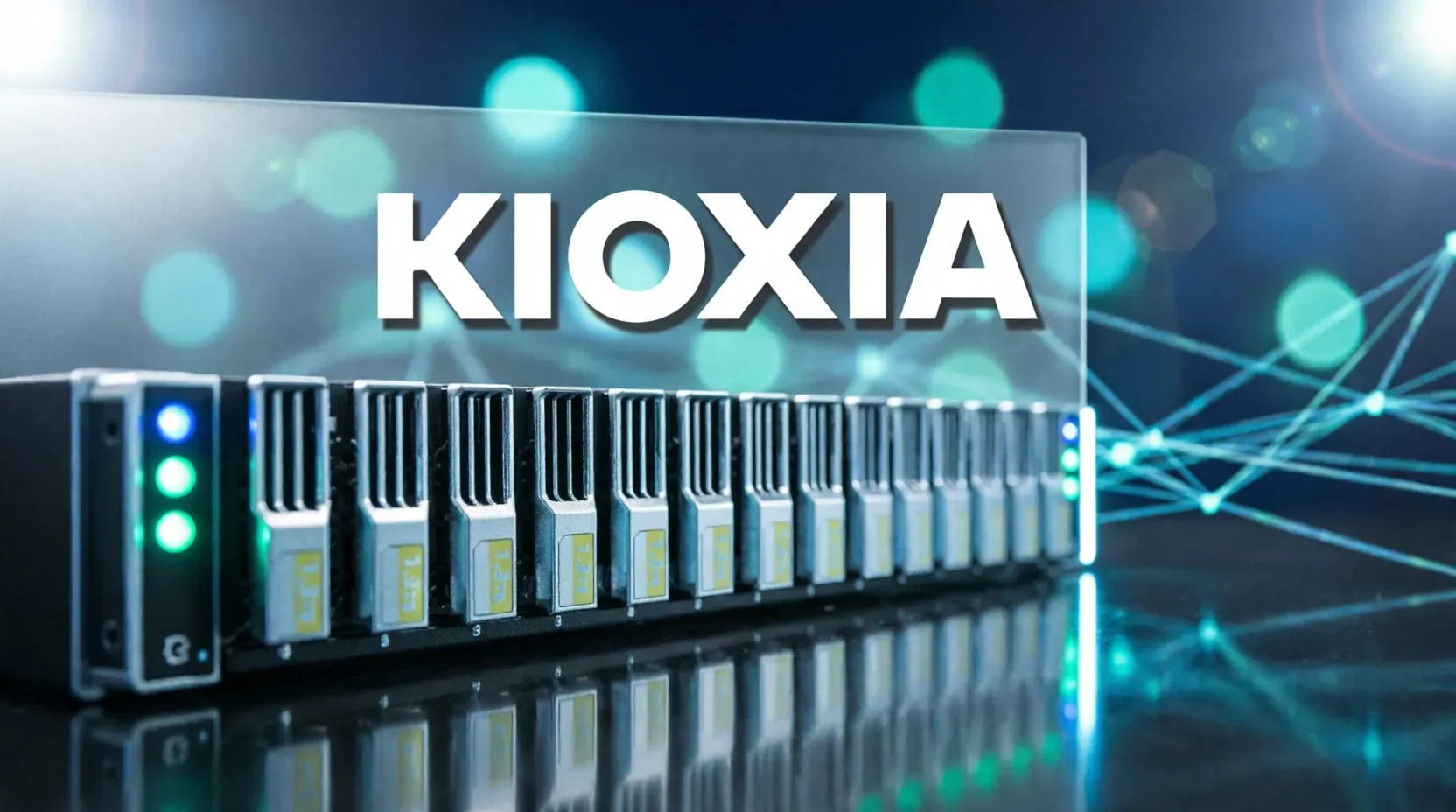
Kioxia Corporation — a world leader in memory solutions — has officially begun shipping samples of its newest 1‑terabit (1 Tb) Triple‑Level‑Cell (TLC) NAND devices. Built on the 10th‑generation BiCS FLASH™ 3D flash architecture, these chips are being fabricated at the state‑of‑the‑art Fab 2 line of the Kitakami Plant in Iwate Prefecture, Japan. The company emphasizes that the samples are intended primarily for functional‑check testing, meaning that early‑stage performance and specification data may differ from the figures that will appear in mass‑production parts. Designed for integration into Kioxia’s enterprise‑ and data‑center‑grade solid‑state drives (SSDs), the devices aim to meet the escalating storage demands of artificial‑intelligence workloads, which require a combination of higher throughput, larger per‑drive capacity, and reduced power draw compared with conventional workloads.
Kioxia Starts Sample Shipments of 10th‑Gen 1 Tb BiCS FLASH Devices
The announcement clarifies that the first batch of 1 Tb TLC samples will be used for functional verification by Kioxia’s internal teams and selected partners. While the baseline technology mirrors that of the 8th‑generation BiCS FLASH™—specifically the CMOS Directly Bonded to Array (CBA) and On‑Pitch Select Gate Drain (OPS) processes—the 10th‑generation implementation pushes key metrics further. Kioxia reports a NAND interface speed of 4.8 Gb/s, representing a 33 % uplift over the previous generation, and a 59 % jump in bit density achieved by stacking 332 layers and improving lateral cell density. In addition, write‑power consumption is claimed to be 18 % lower and read‑power 30 % lower than comparable 8th‑generation parts, a benefit that should translate into measurable energy savings for large‑scale data‑center deployments. The company notes that these figures are derived from a controlled Kioxia test environment; actual performance will depend on host‑device integration, firmware optimization, and real‑world workload characteristics.
Technical Details of the 10th‑Generation BiCS FLASH™
The 10th‑generation architecture relies on two key innovations:
- CMOS Directly Bonded to Array (CBA) – each CMOS wafer and cell‑array wafer is fabricated separately under optimized conditions before being bonded, allowing tighter integration and higher yields.
- On‑Pitch Select Gate Drain (OPS) – this technique shortens the bit line and lowers word‑line capacitance by eliminating unused memory holes, contributing to the reported power‑efficiency gains.
Layer stacking reaches 332 layers, up from earlier generations, and the lateral density improvements raise overall chip density by 59 %. The announced interface speed of 4.8 Gb/s is measured in a specific Kioxia test environment; actual performance may vary with host devices and workloads.
Enterprise Relevance and Product Positioning
Kioxia positions the 10th‑generation devices alongside its existing 9th‑generation line, which targets “high performance at relatively low cost of investing.” The newer generation focuses on “massive capacity and superior performance,” aligning with the storage demands of generative AI and other data‑intensive applications. While the samples are for validation only, the company indicated that the devices will be integrated primarily into its enterprise and data‑center SSD portfolio.
Kioxia’s dual‑axis strategy suggests that customers can choose between cost‑effective 9th‑generation solutions and the higher‑capacity 10th‑generation parts, depending on workload requirements and budget constraints. The announced power‑efficiency improvements could translate into lower operational expenses for data‑center operators, though actual savings will depend on deployment scale and real‑world usage patterns.
Key Takeaways
- Kioxia has begun shipping sample 1 Tb TLC memory devices built on its 10th‑generation BiCS FLASH™ technology.
- The new devices achieve a 4.8 Gb/s NAND interface speed (33 % faster than the 8th generation) and a 59 % increase in bit density by stacking 332 layers.
- Write and read power efficiencies are improved by 18 % and 30 %, respectively, aiming to reduce data‑center power consumption.
TechInsyte's Take
The launch signals Kioxia’s push to meet the storage bandwidth and capacity needs of AI‑driven workloads, while also addressing power constraints in large‑scale deployments. Because the samples are still in a functional‑check phase, enterprises should monitor mass‑production specifications and pricing before committing to refresh cycles. Buyers should watch for detailed performance data and compatibility testing results as Kioxia moves from sampling to full‑scale production.
Source: Businesswire