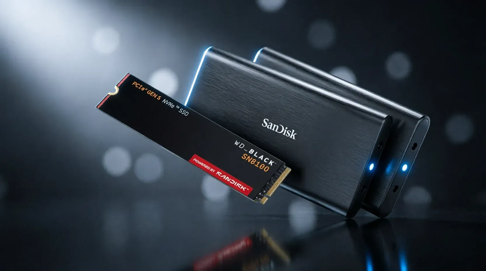
SanDisk (Nasdaq: SNDK) announced that it is now sampling its 1 Tb BiCS10 TLC 3D NAND flash memory, the company’s 10th‑generation NAND product. The new part delivers up to 4.8 Gb/s interface speed, a 59 percent increase in bit density over the BiCS8 generation, and notable power‑efficiency gains—features aimed at data‑intensive and AI‑driven workloads that matter to enterprise IT leaders.
BiCS10 TLC 1 Tb Sampling Milestone
SanDisk said the BiCS10 TLC 1 Tb chip uses advanced lateral scaling to achieve a density greater than 29 Gb/mm², representing a 59 percent improvement in bit density compared with BiCS8. The part supports a NAND interface speed of up to 4.8 Gb/s, a 33 percent increase over the 8th‑generation 3D flash currently in mass production. The architecture adds 332 memory layers and incorporates Toggle DDR6.0, the SCA protocol, and PI‑LTT technology to enable high‑speed, low‑power operation.
Alper Ilkbahar, SanDisk’s CTO, highlighted that “BiCS8 set a new benchmark… With BiCS10 TLC, we build upon that proven foundation to deliver faster interface speeds, higher bit density and improved power efficiency for our customers.” The sampling announcement signals that the product is moving toward volume production, though SanDisk did not disclose a commercial launch date.
Power‑Efficiency Improvements
BiCS10 TLC improves data input/output power consumption by 10 percent for input and 34 percent for output relative to the previous BiCS8 generation. The gains stem from the company’s CMOS Directly Bonded to Array (CBA) process, which fabricates CMOS logic and the memory array on separate wafers before bonding them with high‑precision wafer‑to‑wafer alignment. The reduced power draw is relevant for data‑center operators seeking to lower energy costs while scaling storage capacity.
Potential Enterprise Impact
The combination of higher density, faster interface speed, and lower power use positions BiCS10 TLC for workloads that demand large, fast, and efficient storage—such as AI model training, high‑performance computing, and large‑scale analytics. SanDisk’s control over the full production lifecycle—from design through final assembly—offers supply‑chain resilience, a factor that many CIOs consider when qualifying new flash components. The company did not disclose specific customer pilots or performance benchmarks beyond the quoted figures.
Key Takeaways
- SanDisk is sampling a 1 Tb BiCS10 TLC 3D NAND chip that delivers up to 4.8 Gb/s interface speed, a 33 percent improvement over 8th‑generation 3D flash.
- The new part achieves a 59 percent increase in bit density (greater than 29 Gb/mm²) and adds 332 memory layers compared with BiCS8.
- Input power consumption is reduced by 10 percent and output power by 34 percent versus the prior generation, thanks to the CBA process and PI‑LTT technology.
TechInsyte's Take
The sampling of BiCS10 TLC shows SanDisk is advancing its 3D NAND roadmap to meet the storage bandwidth and efficiency demands of modern data‑center workloads. While the announced performance and power metrics are compelling, the lack of a commercial availability timeline and real‑world benchmark data leaves uncertainty around immediate adoption. CIOs and storage architects should monitor SanDisk’s subsequent product releases and any disclosed customer validation before committing to large‑scale deployments.
Source: Businesswire