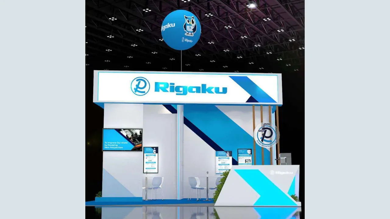
The escalating architectural complexity of high-bandwidth memory (HBM) and advanced logic is forcing a shift in semiconductor inspection strategies toward non-destructive X-ray solutions. Rigaku is positioning itself to address these manufacturing bottlenecks by showcasing a specialized suite of metrology and inspection technologies at SEMICON Taiwan 2026. Scheduled for September 2–4 in Taipei, the company's presence aims to support the critical manufacturing ecosystem in Taiwan, particularly following the 2025 establishment of the Rigaku Technology Center Taiwan (RTC-TW). This strategic move targets the high-precision requirements of modern, multilayered semiconductor devices.
X-ray Solutions for HBM and Advanced Packaging
Rigaku is presenting several technologies designed to manage the transition from traditional wafer-based processes to more complex 2.5D/3D and panel-level packaging (PLP). The XHENA AX-3000 is positioned as a solution for inspecting hidden structures that conventional optical methods struggle to evaluate. By utilizing 3D laminography and automated defect identification, the system aims to provide sub-micron defect detection for micro-bumps and through-silicon vias (TSVs) within CoWoS, HBM, and hybrid bonding environments. Additionally, the XHEMIS WX-PLP310 is being introduced to support process control as the industry shifts toward larger panel formats, measuring material composition and thin-film thickness across large substrates.
To address high-throughput requirements, the company is highlighting the XTRAIA MF Series, specifically the fourth-generation XTRAIA MF-3400 for thin-film analysis and the XTRAIA XD-3300 for ultra-small wafer pad measurements. Furthermore, the ONYX Series is designed to combine X-ray and optical technologies for the non-destructive characterization of complex multilayer structures in BEOL process control. Rigaku is also emphasizing its strategic alliance with Onto Innovation, which seeks to advance hybrid metrology by integrating X-ray and optical capabilities to improve manufacturing precision.
Key Takeaways
- Rigaku will exhibit advanced X-ray metrology solutions at SEMICON Taiwan 2026 from September 2 to 4.
- The XHENA AX-3000 enables sub-micron defect detection for TSVs and micro-bumps in HBM and CoWoS packaging.
- The XHEMIS WX-PLP310 supports the transition to panel-level packaging (PLP) by measuring material composition on large substrates.
TechInsyte's Take
In our view, Rigaku’s focus on HBM and 2.5D/3D packaging signals a direct response to the "visibility gap" created by advanced AI hardware. As chips become more vertically integrated, traditional optical inspection reaches its physical limits, making non-destructive X-ray metrology a necessity rather than an elective upgrade. By deploying specialized tools like the XHENA AX-3000 and the XHEMIS WX-PLP310, Rigaku is attempting to capture the high-growth segment of the supply chain where process control for hybrid bonding and CoWoS is most volatile. Their alliance with Onto Innovation further suggests that the future of semiconductor yield management lies in hybrid metrology—fusing different sensing modalities to solve increasingly opaque manufacturing challenges.
Questions & Answers
How does Rigaku intend to address the limitations of optical inspection in advanced packaging?
Rigaku is positioning its XHENA AX-3000 technology to inspect hidden structures, such as through-silicon vias (TSVs) and micro-bumps, which are difficult to evaluate using conventional optical methods alone through the use of 3D laminography.
What role does the XHEMIS WX-PLP310 play in evolving manufacturing formats?
The XHEMIS WX-PLP310 is designed for panel-level packaging (PLP) process control, allowing manufacturers to measure material composition and thin-film thickness across the larger substrates used in panel formats.
Which specific high-growth semiconductor technologies is Rigaku targeting?
The company is specifically targeting advanced logic, high-bandwidth memory (HBM), 2.5D/3D packaging, CoWoS, and hybrid bonding applications.
What is the strategic significance of the Rigaku-Onto Innovation alliance?
The alliance aims to advance hybrid metrology solutions by combining X-ray and optical technologies, which is critical for the non-destructive characterization of complex, multilayered semiconductor structures.
Source: Businesswire