The transition of quantum technology from fragile, tabletop laboratory instruments to rugged, fieldable enterprise assets is accelerating through a new hardware integration breakthrough. Infleqtion (NYSE: INFQ), Honeywell Aerospace, and UC Santa Barbara (UCSB) have announced the development of a prototype integrated optical “cavity” designed to miniaturize quantum sensors to handheld dimensions. By fabricating this component on a silicon nitride chip at Honeywell Aerospace's photonics foundry, the partners are addressing a primary bottleneck in quantum deployment: the massive physical footprint required for laser stabilization. This development leverages existing semiconductor manufacturing processes, signaling a strategic shift toward high-volume, chip-scale production of quantum-enabled hardware for critical infrastructure and defense applications.
Silicon Nitride Prototyping for Quantum Miniaturization
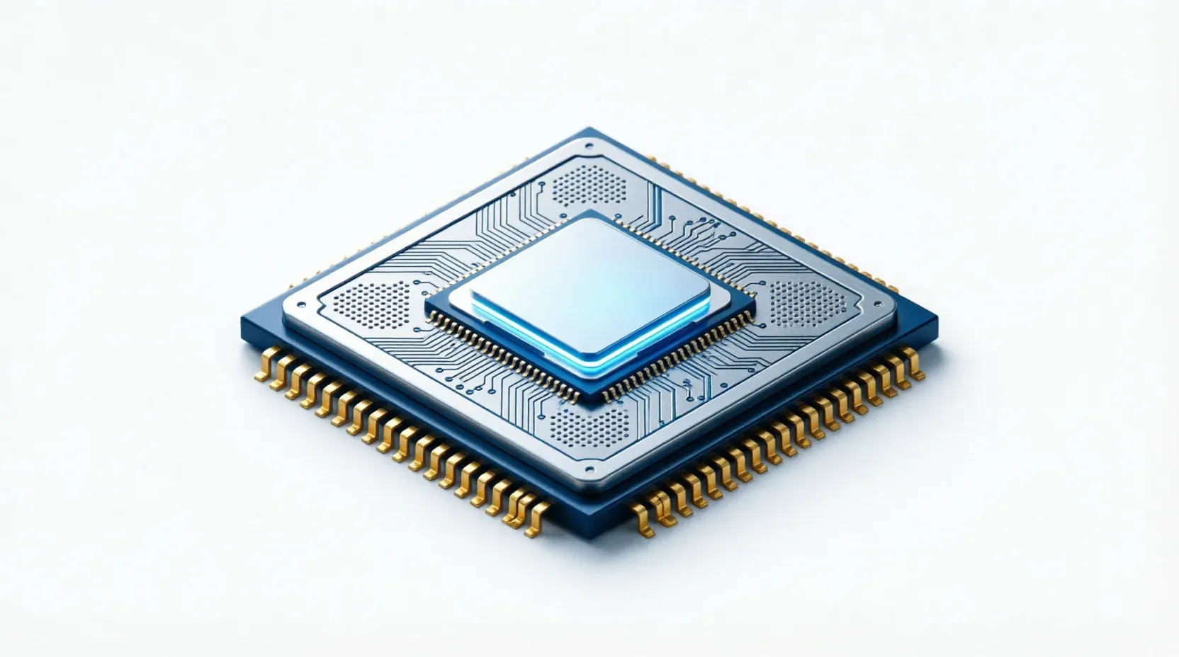
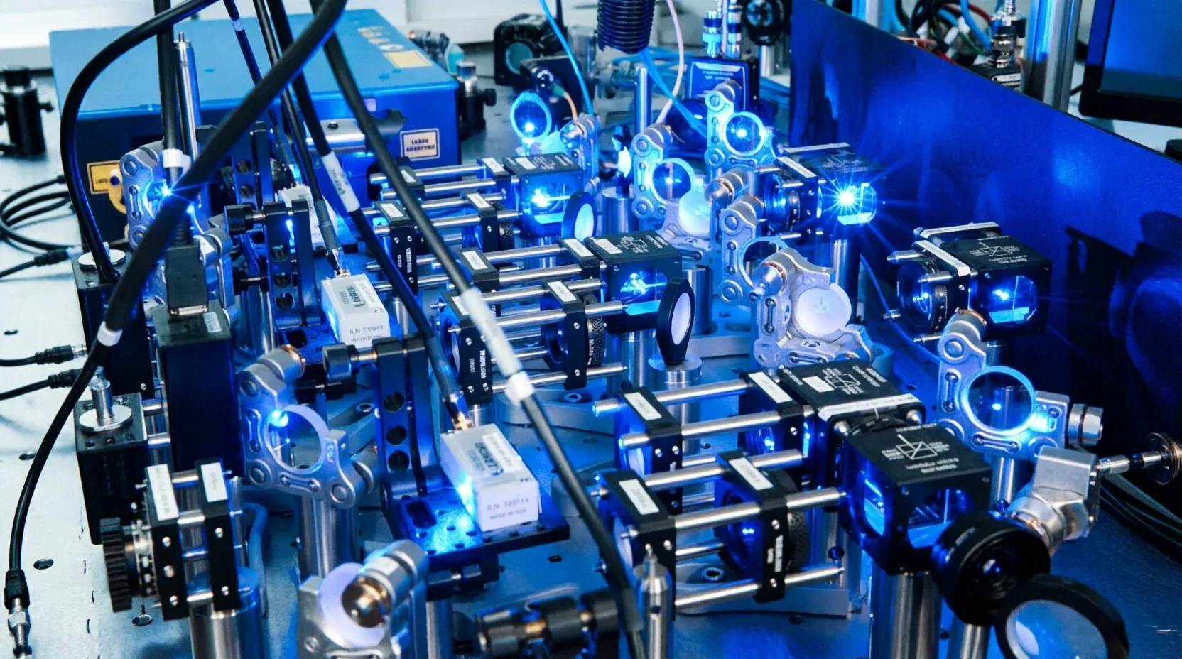
The core of this development lies in the creation of an integrated optical cavity that stabilizes the lasers essential for the precision of quantum computers, clocks, and sensors. Historically, these cavities have functioned as large, delicate instruments that require controlled environments, effectively preventing their use in mobile or field-deployed scenarios. The new prototype, co-designed by Infleqtion’s engineering team and UCSB’s OCAQπ Group, utilizes silicon nitride photonic integration processes developed by Honeywell Aerospace over the last decade. This specific manufacturing approach allows the hardware to be produced within commercial foundries, moving the technology away from bespoke laboratory assembly and toward standardized semiconductor-style mass production.
By shrinking the space required for laser stabilization, the prototype aims to enable the creation of compact quantum systems. Infleqtion CTO Pranav Gokhale noted that the goal is to make these systems smaller, more stable, and manufacturable at scale. The integration of UCSB’s research into Honeywell’s fabrication environment provides a direct pathway to volume production, which is a prerequisite for any technology seeking to move beyond specialized research into widespread commercial or governmental utility. This transition is critical for applications requiring high-precision timing and navigation in environments where traditional, bulky quantum hardware cannot operate.
Scaling Quantum Sensing for Critical Infrastructure
The strategic implications of this chip-scale manufacturing capability extend to several high-stakes enterprise sectors, particularly where precision and reliability are non-negotiable. The partners are positioning this technology to support near-term applications in quantum-enabled precision navigation and atomic timing. For data centers and telecommunications providers, this could mean more resilient synchronization for cell towers and network infrastructure. In the defense and aerospace sectors, the ability to deploy handheld quantum sensors could redefine inertial navigation and sensing capabilities in contested or GPS-denied environments.
The collaboration also highlights a successful model of technology transfer from academia to industry. The photonic technology at the center of this breakthrough was the foundation of SiNoptiq, a startup founded by UCSB’s Professor Daniel J. Blumenthal, which was subsequently acquired by Infleqtion in 2024. This lineage demonstrates how intellectual property managed by UCSB’s Office of Technology & Industry Alliances (TIA) is being converted into scalable hardware. By utilizing Honeywell Aerospace’s state-of-the-art foundry, the group is testing whether the existing global semiconductor infrastructure can be effectively leveraged to bridge the gap between fundamental quantum science and the mass-market requirements of the global telecommunications, energy, and finance industries.
Key Takeaways
- The new integrated optical cavity prototype is fabricated on a silicon nitride chip at Honeywell Aerospace's photonics foundry to reduce the footprint of laser stabilization.
- The manufacturing process utilizes standard semiconductor industry methods, allowing for potential production at scale across existing commercial facilities.
- Target near-term applications for this miniaturized technology include atomic timing for cell towers and data centers, as well as precision navigation.
TechInsyte's Take
In our view, this announcement marks a pivot from "quantum feasibility" to "quantum manufacturability." For years, the enterprise sector has viewed quantum technology as a distant, laboratory-bound prospect due to the extreme sensitivity and scale of the required hardware. By successfully integrating an optical cavity onto a silicon nitride chip using Honeywell Aerospace’s existing foundry processes, this collaboration is attempting to solve the most significant barrier to entry: the supply chain. If these prototypes can indeed be produced in commercial foundries, it removes the "bespoke hardware" tax that has historically stifled quantum adoption. This signals that the industry is moving toward a standardized component model, which is a necessary precursor for the integration of quantum sensing into the broader digital and telecommunications infrastructure.
Questions & Answers
How does this new hardware address the physical limitations of current quantum sensors?
The prototype uses an integrated optical "cavity" fabricated on a silicon nitride chip to reduce the physical space required for laser stabilization. This allows quantum sensors, which were previously large and fragile tabletop instruments, to potentially reach a handheld size suitable for field deployment.
What is the significance of using Honeywell Aerospace's photonics foundry for this project?
Using a commercial foundry means the technology can be produced using manufacturing processes common in the semiconductor industry. This provides a clear path to volume production and widespread deployment, rather than relying on specialized, low-volume laboratory fabrication.
Which enterprise sectors are identified as primary targets for this technology?
The announcement highlights near-term applications in precision navigation and atomic timing. This specifically targets sectors such as telecommunications (for cell towers), data centers, defense, aerospace, energy, and finance.
What role did the acquisition of SiNoptiq play in this development?
SiNoptiq was a startup founded by Professor Daniel J. Blumenthal that specialized in silicon photonics; its acquisition by Infleqtion in 2024 provided the foundational photonic technology that enabled this current collaboration and the development of the silicon nitride chip prototype.
Source: Infleqtion