Avicena is moving its microLED-based optical interconnect technology from theoretical demonstration to active laboratory testing by shipping its 1 Tbps LightBundle evaluation kits (eKits). This shipment marks a transition for the Sunnyvale-based company, providing hyperscalers and AI accelerator developers with hardware to test terabit-class connectivity. By targeting the bandwidth bottlenecks inherent in next-generation AI scaling, Avicena is positioning its laser-free architecture as a potential alternative to traditional copper and silicon photonics for high-density interconnect requirements.
Avicena Deploys 335-Channel MicroLED Arrays
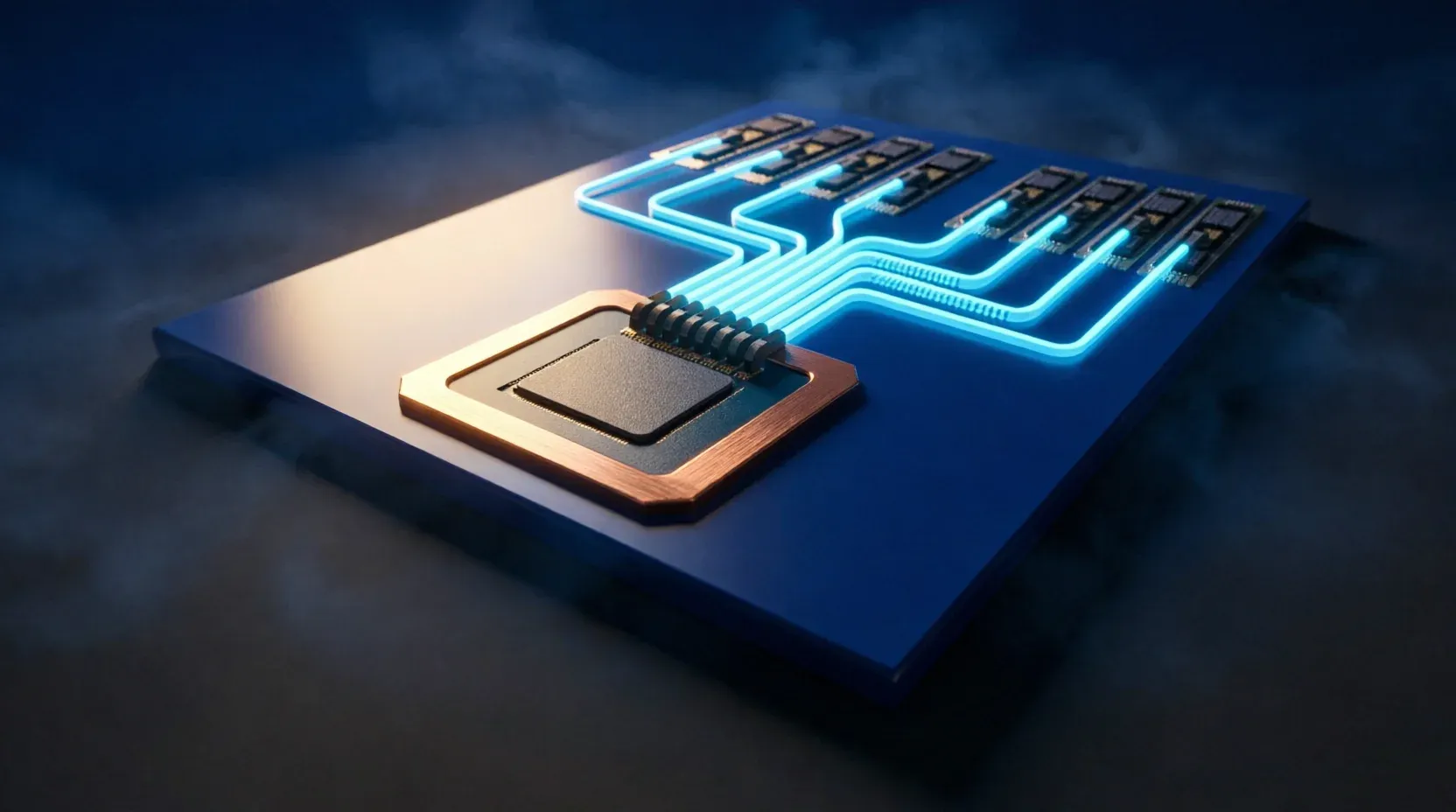
The 1 Tbps LightBundle eKit utilizes a specialized architecture designed to bypass the limitations of conventional laser-based optical solutions. The hardware incorporates a 335-channel microLED array, where each individual data channel operates at up to 3 Gbps. This array is coupled via an Avicena multicore fiber bundle to a 335-element integrated photodiode array. This configuration aims to deliver an aggregate raw throughput of 1 Tbps.
The company is marketing this laser-free approach as a way to achieve high bandwidth density and low power consumption while maintaining robust operation at elevated temperatures. To facilitate engineering evaluations, the eKit includes host interface boards, integrated diagnostics, and a graphical user interface. These tools allow developers to characterize critical performance metrics, including optical signal integrity, link budgets, eye quality, crosstalk, power efficiency, and bit error rate performance. This enables a comprehensive assessment of how microLED technology performs within specific AI infrastructure environments.
Addressing AI Scale-In and Scale-Up Bottlenecks
As AI systems demand higher bandwidth between accelerators, memory, and switch fabrics, traditional copper interconnects face increasing difficulties regarding reach, routing density, and energy efficiency. Avicena is positioning LightBundle to address these specific constraints across various connectivity layers. The technology is intended for both scale-in and scale-up applications, specifically targeting die-to-die, die-to-memory, XPU-to-XPU, XPU-to-CPU, and XPU-to-switch links.
By replacing standard lasers with dense microLED transmitter arrays, the platform seeks to provide flexible reach that extends beyond the practical limits of copper. This development targets a broad spectrum of the semiconductor and data center ecosystem, including AI accelerator developers, memory manufacturers, networking companies, and system architects. The availability of these eKits allows these entities to evaluate whether microLED-based connectivity can meet the rigorous power and reliability demands of next-generation AI scale-in and scale-up architectures.
Key Takeaways
- Avicena has begun shipping 1 Tbps LightBundle evaluation kits featuring 335 microLED channels operating at 3 Gbps each.
- The technology utilizes a laser-free architecture consisting of a microLED array coupled via multicore fiber to an integrated photodiode array.
- The eKit provides diagnostic tools for evaluating signal integrity, link budgets, eye quality, crosstalk, power efficiency, and bit error rate.
TechInsyte's Take
In our view, Avicena’s move to ship 1 Tbps evaluation kits signals a critical attempt to challenge the dominance of silicon photonics and copper in the AI data center. By removing the laser from the equation, Avicena is betting that microLEDs can solve the thermal and power density crises currently facing XPU-to-XPU and die-to-memory interconnects. If these kits prove that microLEDs can maintain signal integrity at scale while operating at high temperatures, it could fundamentally alter the roadmap for AI hardware architecture. This is no longer just a research project; it is a direct play for the physical layer of the AI era.
Questions & Answers
How does the LightBundle architecture differ from conventional optical solutions?
Unlike conventional solutions that rely on lasers and silicon photonics, LightBundle uses a laser-free architecture. It employs dense microLED transmitter arrays coupled through a multicore fiber bundle to integrated photodetector arrays to achieve high bandwidth density.
What specific connectivity use cases is Avicena targeting with these kits?
The company is targeting high-density links essential for AI scaling, including die-to-die, die-to-memory, XPU-to-XPU, XPU-to-CPU, and XPU-to-switch connectivity for both scale-in and scale-up applications.
What technical metrics can engineers evaluate using the LightBundle eKit?
Engineering teams can use the kit's integrated diagnostics and graphical user interface to characterize optical signal integrity, link budgets, eye quality, crosstalk, power efficiency, and bit error rate performance.
What is the maximum throughput capacity of the current LightBundle eKit?
The latest LightBundle eKit provides an aggregate raw throughput of up to 1 Tbps, achieved through 335 microLED channels operating at up to 3 Gbps each.
Source: Businesswire