
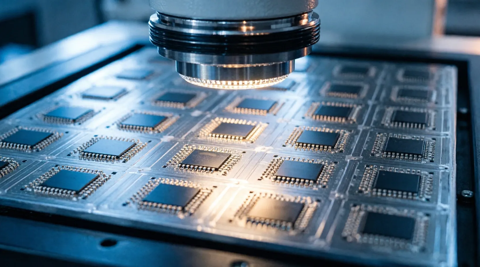
Atomica, a U.S.-based microfabrication foundry, has announced the launch of its AI Optical Source Platform to address critical physical bottlenecks in AI infrastructure. As AI clusters scale from thousands to hundreds of thousands of accelerators, traditional electrical interconnects face increasing limitations in bandwidth, reach, and thermal load. This new platform enables customers to develop compact laser sources, optical engines, and thermally stable optical interconnects, providing the necessary microfabricated structures to manage optical power within dense, next-generation AI hardware environments.
Atomica's New Microfabrication Platform for Optical Sources
The AI Optical Source Platform is designed to help developers bridge the gap between advanced optical architectures and manufacturable hardware. It focuses on the specific challenges of generating, stabilizing, coupling, and managing optical power in compact, reliable packages. This launch complements Atomica's existing AI Optical Connectivity Platform, which focuses on routing and integrating light. While the connectivity platform handles light routing and alignment, the new source platform addresses the generation and stabilization of that light.
The platform supports a wide range of microfabricated structures, including external laser source modules, compact laser boxes, and laser-to-fiber coupling modules. It also facilitates the production of silicon photonics fiber attach assemblies, photonic integrated circuit packaging, and optical transceiver subassemblies. By providing specialized manufacturing approaches for high-density optical subsystems, Atomica aims to solve the "laser source bottleneck," ensuring stable optical power delivery without adding unacceptable heat, drift, or alignment loss to dense AI optical systems.
Addressing Physical Bottlenecks in Scaling AI Clusters
As AI infrastructure scales, the physical layer faces significant challenges. In emerging co-packaged or near-package optics architectures, the optical engine sits near the switch ASIC, GPU, or accelerator, while the laser source may be located separately for thermal and reliability reasons. This separation introduces complexities in maintaining sub-micron coupling and mechanical stability. Atomica's platform addresses these needs by providing manufacturing processes for silicon optical benches, V-grooves, microlenses, and thermal isolation structures.
The platform is positioned to support various high-density components, such as high-density fiber array units, optical switching modules, and LiDAR subsystems. According to Atomica CEO Eldon Klaassen, the primary challenge lies in managing heat, preventing drift, and maintaining sub-micron coupling to ensure reliable optical power for years. By focusing on process repeatability and assembly tolerances, the platform aims to turn promising optical designs into scalable, manufacturable hardware for the evolving AI hardware stack.
Key Takeaways
- Atomica's new platform addresses the "laser source bottleneck" by enabling the manufacture of compact, stable, and reliable laser source systems.
- The platform supports diverse components, including silicon photonics fiber attach assemblies, optical transceiver subassemblies, and high-density fiber array units.
- The launch complements Atomica's AI Optical Connectivity Platform, which focuses on the alignment, packaging, and integration of light.
TechInsyte's Take
In our view, Atomica is strategically positioning itself at a critical junction in the AI hardware supply chain. As electrical interconnects reach their physical limits regarding bandwidth and power consumption, the industry's shift toward optical connectivity is inevitable. However, the transition depends heavily on moving beyond theoretical photonic designs to mass-manufacturable hardware. By focusing on the microfabrication of laser sources and coupling structures, Atomica is targeting the specific physical-layer hurdles—such as thermal drift and sub-micron alignment—that currently prevent widespread adoption of advanced co-packaged optics. This move signals that the next phase of AI scaling will be defined by microfabrication precision.
Source: Prweb