Toshiba Electronic Devices & Storage Corporation announced that it has started shipping test samples of its new 1200 V trench‑gate silicon‑carbide (SiC) MOSFET, part number TW007D120E. The device is targeted at power‑supply systems for next‑generation AI data centers and is also positioned for renewable‑energy equipment such as photovoltaic inverters and EV chargers. Toshiba plans mass production in fiscal year 2026.
What Was Announced
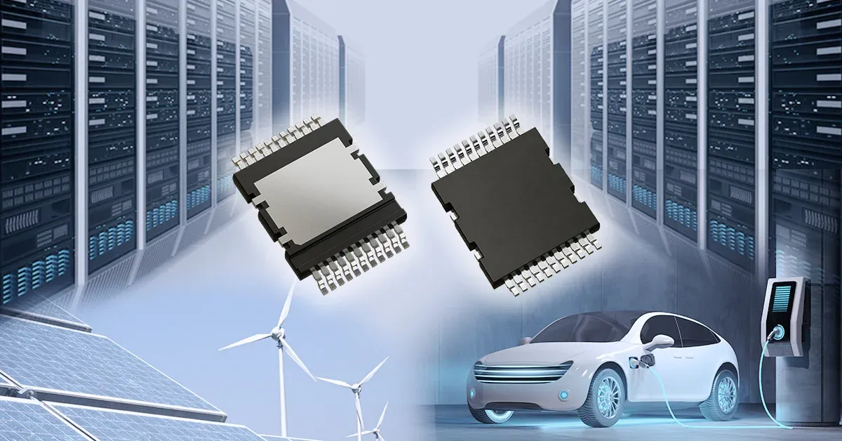
The company is now providing test samples of TW007D120E, a 1200 V SiC MOSFET built on Toshiba’s proprietary trench‑gate structure. Compared with Toshiba’s current 3rd‑generation SiC MOSFET (TW015Z120C), the new part reduces on‑resistance per unit area (RDS(on)A) by roughly 58 % and improves the figure of merit (RDS(on) × Qgd) by about 52 %. The device is packaged in a QDPAK that supports top‑side cooling, enabling higher power density and better thermal performance. Key electrical specs include a typical RDS(on) of 7 mΩ at VGS = 15 V, gate‑drive voltage of 15‑18 V, and a drain current rating of 172 A at 25 °C.
The product derives from research results of project JPNP21029, which was subsidized by Japan’s New Energy and Industrial Technology Development Organization (NEDO). Toshiba indicated that it will expand the SiC MOSFET lineup beyond data‑center power supplies to automotive applications.
Where It Fits
Generative AI workloads are driving higher power consumption in data centers, prompting a shift toward 800 V high‑voltage DC (HVDC) architectures. Higher‑efficiency power conversion is essential to control operating costs and thermal constraints. By offering lower conduction and switching losses, TW007D120E can improve overall system efficiency and reduce heat generation, supporting the miniaturization of power‑supply modules.
Beyond AI servers, the device’s specifications make it suitable for photovoltaic inverters, uninterruptible power supplies (UPS), EV charging stations, energy‑storage systems, and industrial motors. The QDPAK package’s top‑side cooling aligns with the need for compact, high‑density power stages in these applications.
Operational Relevance
For CIOs and data‑center operators, the MOSFET’s reduced RDS(on)A translates into measurable energy savings, especially at scale. Lower switching loss also eases thermal design, potentially allowing higher power‑density designs without additional cooling infrastructure. The 15‑18 V gate‑drive requirement fits within existing driver ecosystems, simplifying integration.
In renewable‑energy deployments, the same efficiency gains can improve inverter performance and lower the levelized cost of electricity. For EV charging stations and UPS units, the higher voltage rating (1200 V) and robust current capability (172 A) enable more compact converters while maintaining reliability.
What To Watch
- Mass‑Production Timeline: Toshiba targets fiscal year 2026 for volume production. Buyers should monitor the ramp‑up schedule and availability of the QDPAK package.
- Automotive Extension: The company plans to develop related trench‑gate SiC MOSFETs for automotive use. Follow announcements for specifications and qualification milestones.
- Competitive Landscape: Other SiC vendors are also advancing 1200 V devices. Comparative performance data will be critical for procurement decisions.
- Regulatory Impact: Improved efficiency may help data‑center operators meet tightening energy‑use regulations in key markets.
Key Takeaways
- Toshiba began shipping test samples of the 1200 V trench‑gate SiC MOSFET TW007D120E, aimed at AI data‑center power supplies and renewable‑energy equipment.
- The device reduces on‑resistance per unit area by ~58 % and improves the RDS(on) × Qgd figure of merit by ~52 % versus Toshiba’s prior 3rd‑generation SiC MOSFET.
- Mass production is planned for fiscal year 2026, with future extensions to automotive applications.
TechInsyte's Take
Toshiba’s TW007D120E addresses a concrete efficiency bottleneck in high‑power AI data centers, where even modest reductions in conduction and switching loss can yield significant cost and carbon‑footprint benefits at scale. The trench‑gate architecture and top‑side‑cooled QDPAK package provide a practical path to higher power density without redesigning existing driver circuits. Decision‑makers should evaluate sample performance against current SiC offerings and consider the device’s suitability for both data‑center and renewable‑energy deployments. The upcoming 2026 mass‑production window and the company’s stated intent to broaden the product line into automotive markets suggest a longer‑term strategic push in SiC technology, but buyers will need to watch for final qualification data and supply‑chain readiness before committing to large‑scale adoption.
Source: Businesswire