TeraSignal is attempting to solve the escalating power and latency penalties inherent in scaling AI infrastructure by moving signal processing from the digital to the analog domain. The company has introduced its Analog Wave Processor (AWP) architecture, designed to handle mathematical operations directly on broadband electrical waveforms. This development targets the critical transition toward 200G per lane connectivity required for 1.6T and 3.2T AI systems.
AWP Architecture and Wave-Domain Processing
The AWP architecture departs from conventional digital signal processing (DSP) or standard analog equalizers that rely on digitized samples. Instead, TeraSignal is positioning AWP to perform weighting, delay, and accumulation directly on broadband waveforms. This wave-domain approach is intended to provide sophisticated signal processing while maintaining the low-power and low-latency benefits of linear interconnects. Specifically, the technology aims to provide linear amplitude and phase response across wide bandwidths and equalization that extends beyond the Nyquist frequency to address high-frequency channel impairments. By utilizing wave-domain feed-forward equalization (FFE), the architecture seeks to correct precursor and postcursor inter-symbol interference (ISI) and mitigate reflections through weighted and delayed waveform processing.
Integrating TSLink with the Lotus Platform
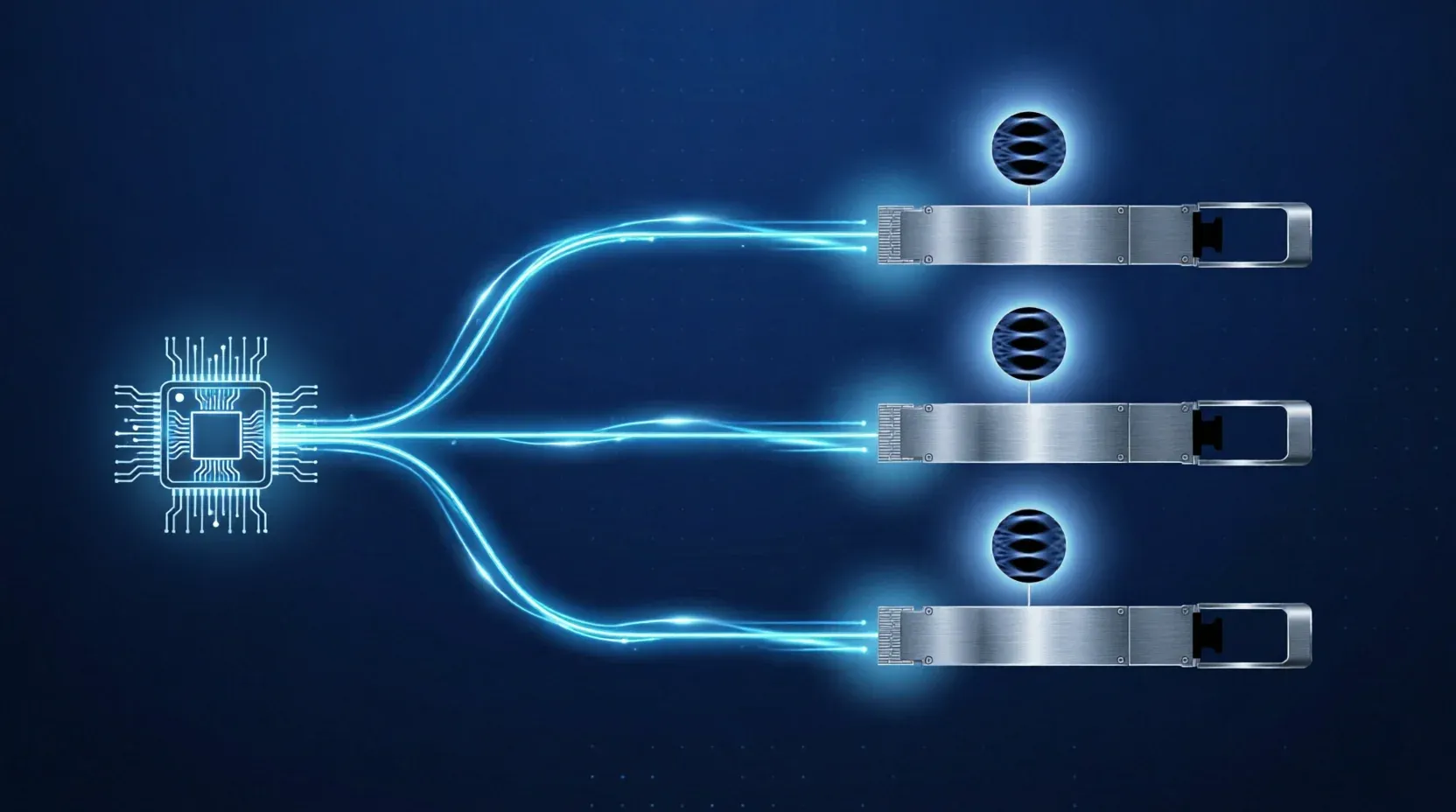
TeraSignal is linking this new processing capability with its TSLink technology to create what it describes as an intelligent closed-loop connectivity architecture. While TSLink measures and identifies channel conditions, AWP provides the corrective wave-processing capabilities. This combination is designed to increase link margin and extend the reach of DSP-free linear interconnects by leveraging the OIF’s CMIS-LT protocol. The AWP is being integrated into the company's Lotus 200G/lane product family, which includes the TS5802 copper redriver, the TS8802 linear MZM driver, and the TS9802 linear TIA. This suite is intended to support a variety of AI interconnect applications, including copper and optical configurations such as ACC, LPO, NPO, and CPO.
Key Takeaways
- TeraSignal introduced the Analog Wave Processor (AWP) to perform mathematical operations directly on broadband electrical waveforms.
- The AWP architecture is designed for 200G/lane connectivity to support 1.6T and 3.2T AI infrastructure.
- The technology is integrated into the Lotus 200G/lane family, including the TS5802, TS8802, and TS9802 components.
TechInsyte's Take
In our view, TeraSignal is betting that the industry's move toward 200G/lane will make traditional DSP-based architectures too power-hungry for massive AI scale-up clusters. By moving processing into the analog wave domain, the company is attempting to bypass the "digital tax" of latency and energy consumption. If AWP can successfully mitigate impairments without the overhead of digitization, it could become a vital component for operators balancing the extreme bandwidth demands of 3.2T systems against strict thermal and power envelopes in the data center.
Questions & Answers
How does AWP differ from traditional DSP-based architectures?
Unlike traditional DSP architectures that operate on digitized samples, AWP performs weighting, delay, and accumulation directly on broadband electrical waveforms in the analog domain to preserve low power and low latency.
What specific AI infrastructure scales is this technology targeting?
The AWP is designed for 200G/lane connectivity, which is intended to support the requirements of 1.6T and 3.2T AI infrastructure.
How does the combination of AWP and TSLink function?
TSLink acts as the intelligence layer that measures and identifies link and channel conditions, while AWP provides the wave-processing capabilities necessary to compensate for those identified impairments.
Which specific product components comprise the Lotus 200G/lane platform?
The platform includes the TS5802 copper redriver, the TS8802 linear MZM driver, and the TS9802 linear TIA.
Source: Businesswire