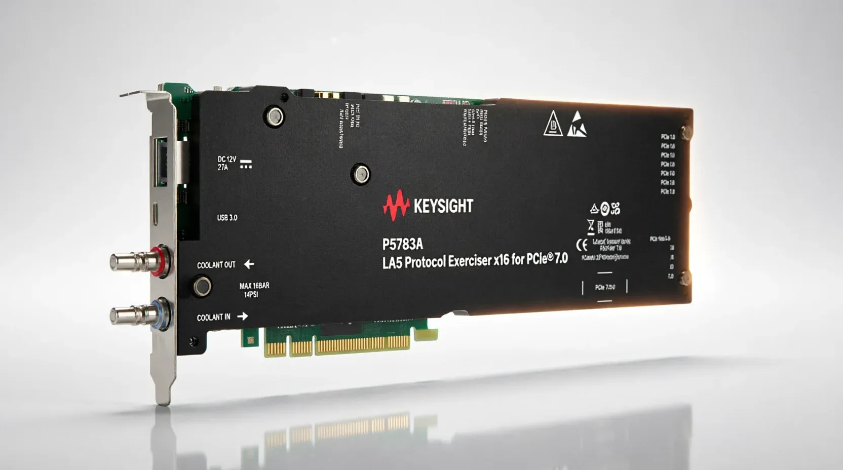
The escalating bandwidth requirements of artificial intelligence workloads are forcing a rapid transition toward higher-speed interconnects, creating a critical validation bottleneck for data center hardware. Keysight Technologies has introduced its Protocol Test Solution for PCIe 7.0 to address this shift, providing an integrated platform designed to validate next-generation devices at the protocol layer. By targeting the 128 GT/s raw data rate, the company aims to help engineering teams manage the increased complexity of link establishment and interoperability in rack-scale systems. This development arrives as PCIe 7.0 is expected to become the dominant interconnect for connecting GPUs, accelerators, switches, memory, and storage within AI-driven architectures, necessitating more robust debugging tools to prevent costly late-stage silicon redesigns.
Validating the 128 GT/s PCIe 7.0 Interconnect
As AI workloads drive demand for massive compute and data bandwidth, the PCIe 7.0 standard doubles the raw data rate to 128 GT/s. This performance leap introduces significant technical hurdles for engineers, particularly regarding link establishment, protocol behavior, and interoperability across increasingly complex architectures. Keysight is positioning its new solution as a method to mitigate these risks by providing deep visibility into the protocol layer during the critical bring-up phase. The platform is designed to allow engineers to investigate Link Training and Status State Machine (LTSSM) behavior, FLIT-based encoding, and complex transaction layer issues.
The solution functions as a combined protocol analyzer and exerciser, integrated with a dedicated test platform and analysis software. This setup is intended to provide a "link partner" for device bring-up, allowing early adopters to move from initial silicon validation through to full interoperability and compliance testing. By enabling "instant link-up," Keysight claims the architecture allows for stable analysis without the need for manual analyzer tuning. This capability is aimed at helping development teams identify protocol errors and transaction layer packet issues earlier in the lifecycle, which the company suggests can reduce the likelihood of schedule delays or the need for hardware redesigns during the final stages of system development.
Scaling AI and Data Center Infrastructure
The deployment of PCIe 7.0 is closely linked to the evolution of rack-scale systems, where high-speed interconnects must reliably manage communication between diverse components like accelerators and storage. Keysight’s solution is being marketed as a tool to advance AI infrastructure development by supporting these high-density architectures while maintaining backward compatibility. This compatibility is intended to protect existing test investments and ease the migration path for enterprises moving toward next-generation scale-up designs.
The strategic importance of this validation capability is highlighted by industry collaboration. Synopsys, which provides PCIe 7.0 IP solutions, noted that establishing a reliable link at 128 GT/s between production silicon and test equipment is a vital interoperability milestone. According to Synopsys, the ability to validate silicon-proven IP with Keysight’s protocol solution allows customers to commit to AI and data center designs with higher confidence. Keysight intends to demonstrate the Protocol Test Solution for PCIe 7.0 at the OCP Global Summit in San Jose, California, scheduled for October 13-16, 2026. This timeline suggests a long-term focus on the maturation of the PCIe 7.0 ecosystem as it moves from early silicon validation toward widespread data center adoption.
Key Takeaways
- Keysight's new PCIe 7.0 Protocol Test Solution supports a raw data rate of 128 GT/s to meet AI and data center bandwidth demands.
- The integrated platform combines a protocol analyzer, exerciser, test platform, and analysis software to facilitate device bring-up and compliance testing.
- The solution is designed to provide visibility into LTSSM transitions, FLIT-based encoding, and transaction layer packet transactions to accelerate debugging.
TechInsyte's Take
In our view, Keysight’s move into PCIe 7.0 testing is a direct response to the "complexity tax" imposed by the AI hardware boom. As data rates double to 128 GT/s, the margin for error in signal integrity and protocol handshake becomes razor-thin. We see this not just as a product launch, but as a necessary infrastructure play; without reliable validation tools, the deployment of next-generation GPU clusters and AI accelerators could face significant delays due to interoperability failures. By partnering with IP providers like Synopsys, Keysight is attempting to lock in its position at the center of the hardware development lifecycle. For enterprise IT leaders, this signals that the underlying fabric of the data center is about to undergo a massive, high-speed upgrade that will require much more sophisticated testing and validation protocols than previous generations.
Questions & Answers
How does the PCIe 7.0 protocol impact AI and data center hardware requirements?
PCIe 7.0 doubles the raw data rate to 128 GT/s, which is essential for the high-bandwidth demands of AI workloads. It is expected to become the primary interconnect for rack-scale systems, facilitating high-speed communication between GPUs, accelerators, memory, and storage.
What specific technical challenges does the Keysight solution aim to resolve?
The solution targets the difficulties of validating link establishment, protocol behavior, and interoperability at 128 GT/s. Specifically, it provides visibility into LTSSM behavior, FLIT-based encoding, and transaction layer packet transactions to help engineers isolate errors before they cause redesigns.
What is the strategic benefit of the integrated analyzer and exerciser workflow?
The integrated workflow provides a consistent environment from initial silicon bring-up through to interoperability and compliance testing. This is intended to reduce early silicon risk by uncovering protocol issues sooner, thereby shortening development cycles and minimizing late-stage rework.
How does this technology protect existing enterprise test investments?
The solution includes backward compatibility, which Keysight suggests allows engineers to validate next-generation scale-up architectures while easing the migration process and protecting previous investments in testing infrastructure.
Source: Keysight