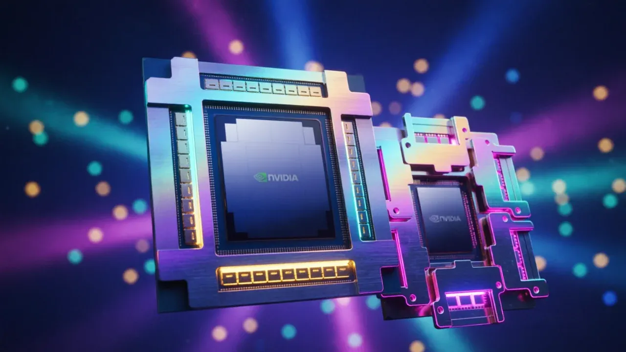

Cadence and Samsung Foundry announced a multi‑year agreement to broaden their collaboration on Samsung’s second‑generation 2nm process. The deal adds Memory and Interface IP—including NVIDIA NVLink‑C2C—and certifies Cadence’s AI‑optimized EDA and SDA flows for advanced AI, HPC and physical‑AI designs across data‑center, edge and intelligent‑device markets.
Cadence‑Samsung Foundry 2nm Collaboration Details
The new agreement expands the Cadence® portfolio of Memory and Interface IP to cover high‑speed SerDes, PCIe®, UCIe® and all leading memory interfaces on the second‑generation 2nm node. It also adds NVIDIA NVLink‑C2C‑enabled interconnect and CUDA‑X GPU‑accelerated libraries. Certified Cadence flows now include Innovus™ Implementation, Virtuoso® Studio, Integrity™ 3D‑IC Platform, Voltus™ Power Integrity, Quantus™ Extraction and Tempus™ Timing, providing a sign‑off‑ready platform for AI infrastructure and physical‑AI designs.
Cadence’s tools enable key 2nm design features such as glitch‑power optimization in place‑and‑route and a smart hierarchical flow to improve performance, power and area (PPA) while reducing turnaround time. Samsung’s 3D Cube‑H design is supported through a full system‑planning and verification flow that incorporates silicon‑interposer auto‑routing, Cadence Cerebrus® Intelligent Chip Explorer, and Pegasus™ Verification.
NVIDIA and Ambarella Leverage the Expanded Platform
NVIDIA’s vice president of computational engineering, Timothy Costa, said the partnership allows NVIDIA to use Cadence’s GPU‑accelerated design flows on Samsung’s 2nm platform to optimize performance and delivery of next‑generation AI architectures and high‑bandwidth interconnects.
Ambarella’s chief operating officer, Chan Lee, highlighted the importance of the co‑optimized IP and tools for its upcoming 2nm edge AI SoC, which targets robotics, drones and other intelligent‑edge applications. The collaboration provides Ambarella with a sign‑off‑ready IP and design kit that reduces risk and supports low‑power AI perception and physical‑AI workloads.
Platform Visibility at SAFE 2026
Cadence and Samsung Foundry will showcase the enhanced partnership at the Samsung Advanced Foundry Ecosystem (SAFE) 2026 event, featuring technical sessions and demonstrations of second‑generation 2nm and 3D‑IC design flows for GPU‑accelerated AI workloads.
Key Takeaways
- The multi‑year deal adds Memory and Interface IP—including NVIDIA NVLink‑C2C—and expands Cadence’s certified AI‑optimized EDA/SDA flows for Samsung’s second‑generation 2nm node.
- Certified Cadence tools now cover the full design stack—from digital implementation (Innovus) to analog/custom (Virtuoso) and 3D‑IC planning (Integrity) – enabling sign‑off‑ready AI and HPC designs.
- NVIDIA and Ambarella are among the early adopters, using the platform to accelerate high‑bandwidth interconnects and low‑power edge AI SoCs, respectively.
TechInsyte's Take
The expanded Cadence‑Samsung Foundry partnership delivers a more complete, sign‑off‑ready design ecosystem for the emerging 2nm node, which could ease the engineering burden for AI‑focused silicon projects. Buyers should monitor how quickly ecosystem partners adopt the new IP and whether the promised performance‑per‑watt gains materialize in silicon shipments.
The partnership is set to shape the next wave of AI‑centric silicon, and industry watchers will be keen to see how quickly the promised design efficiencies translate into real‑world silicon deliveries.
Source: Businesswire